Fumio S. Ohuchi
Professor Emeritus
Materials Science & Engineering
Adjunct Professor
Physics
- ohuchi@uw.edu
- (206) 685-8272
- ROB 315
- Faculty Website
- Ohuchi Group
- PNNL/UW Joint Institute for Nanoscience
- Durint Biomimetics
Biography
Fumio Ohuchi’s research focuses on the physical and chemical processes involved in epitaxial growth dissimilar materials, as well as the synthesis, characterization and transport properties of the Group VI compounds (oxide, sulfides, selenides, and telluride) thin film materials. He is an adjunct professor in Physics, and has developed collaborative curriculum in nanoscience between UW and PNNL, and is passionate about further developing international relationships for UW materials researchers and educators.
Ohuchi has held leadership roles in the UW Department of Materials Science & Engineering as interim department chair, associate chair, and undergraduate program coordinator.
Education
- Ph.D., Materials Science & Eng., University of Florida, Gainesville, Florida, 1981
- M.S., Physics, Sophia University, Tokyo, Japan, 1974
- B.S., Physics, Sophia University, Tokyo, Japan, 1972
Previous appointments
- Interim UW MSE Department Chair, 2016-17
- Visiting scholar at Hahn Meitner Institute, Berlin, Germany, 1987
- NORCUS Professorship at the Battle Pacific Northwest Lab., Richland, WA.
Research Statement
Understanding physical and chemical processes at dissimilar material interfaces Materials technology in the next generation relies on the manipulation and control of atoms and molecules at surfaces and interfaces. Understanding physical and chemical processes at the material's surfaces and dissimilar interfaces is an overall theme of Dr. Ohuchi's research over the past two decades. His primary research is focused on:
- Physical and chemical processes involved in epitaxial growth dissimilar materials
- Synthesis, characterization and transport properties of the Group VI compounds (oxide, sulfides, selenides, and telluride) thin film materials.
Dr. Ohuchi has been involved in a new type of material development strategy called "Combinatorial Materials Exploration (CME)" in collaboration of Dr. Chikyow of National Institute of Materials Science, Tsukuba, Japan. CME as a new research approach to explore an extremely large multi-variant materials space is rapidly becoming a new paradigm for accelerated materials research by enabling both screening and understanding complex material systems in a time- and cost-effective manner. He is now using this technique to explore electrically conductive transition metal oxides for electronic use. His work has recently been published [2.10-1]. Currently he is building his new CME laboratory at the University of Washington. Systematic variance of properties with material's composition or processing parameters yields information on nanoscale mechanisms underlying structure-property relationships; for example changing average valence or atomic separation [3.1, 3.2, 2.15-11]. He believes that successful application of CME to critical problems in the microelectronics area facilitates further advancement of inorganic materials science programs as a whole.
Brief Summary of Dr. Ohuchi's Recent Research (2005-2006)
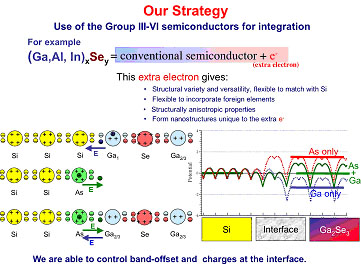
Our research group is investigating how various materials are integrated into "Si". The following two charts explain our strategy of approach, and the type of materials currently working.


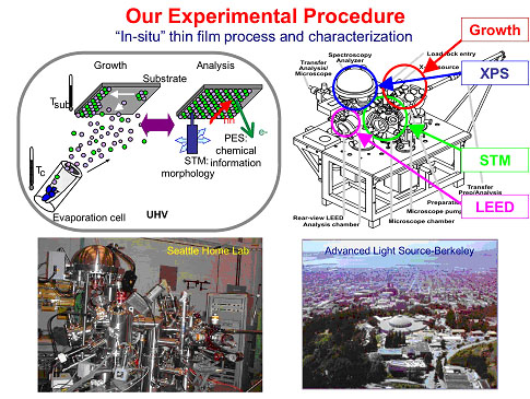
Our experimental approach is rather unique. Since "intrinsic properties" of the interface often control entire process of the electronic devices, we fabricate materials and characterize "in-situ". Our experimental facility, shown below, consists of material-growth followed by "in-situ" characterization by various surface science tools, such as XPS, LEED, ISS, STM, AFM and STS.

Introducing our recent research activities, I will use the following two examples. First example is research related to a search for new silicon compatible semiconducting materials, and their interfaces. Silicon has been the backbone of modern microelectronics, and will likely remain so. Successful expansion of silicon technology to the next generation will require combining other crystalline materials with silicon through heteroepitaxy. Integration of conventional semiconductor materials, such as III-V (such as GaAs) and II-VI (such as ZnSe), to silicon has been demonstrated; however, our approach is very different from those: We have chosen unique materials known as Group III-VI compound, as represented by Ga-Se, Al-Se and In-Se. Stoichiometrically, these materials takes a form of III2VI3. For example, Ga2Se3 can be written as Ga3-1Se3, implying that every third of Ga site becomes 'vacant'. We have shown that these vacancies are perfectly lined up epitaxially, and controlled subsequent crystal structure. We named this growth as "vacancy-induced-growth" and published in PRL 2005.

The group III-VI compounds are also considered as "conventional semiconductor PLUS extra electron system". For example, "Ga-Se" is considered as a material with "(Ga)-(As plus extra electron)", or "(Zn plus extra electron)-(Se)" (see periodic table). Having this extra electron in our system, we are able to control various electronic properties, such as band-offset and dipole formation at the interface. This is shown in the next view graph. Our research focuses on the basic physics and materials science of these new materials and the bridge to new technologies. I believe such long range, exploratory materials development, is essential to expanding America's technology base.

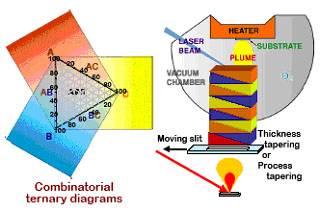
Our second area of research is to investigate transport properties of the transition metal oxides. Recent technology demands a use of materials at extreme conditions, such as high temperature, high pressure, high radiation environments. Oxides are inherently sustainable to those conditions. Electrical and thermal transport properties are most fundamental ones among various properties, yet difficult to study. Shown below an example from NiO-CuO-Mn2O3 ternary oxide system, where we are searching compositions that give good electrical conductivity. For this, we are using an intelligent way of searching new materials, called "Combinatorial Materials Exploration". Thin films are fabricated using a pulsed laser deposition technique, where the materials are alternatively deposited in a tapered shape from three directions, ultimately forming a ternary diagram shown above. This sample (combinatorial library) contains all possible ternary and binary compositions on "one wafer", so that the property related to specific compositions can be probed using appropriate techniques. This is illustrated below.


Select publications
- Benjamin W. Krueger, Christopher S. Dandeneau, Evan M. Nelson, Scott Dunham, Fumio S. Ohuchi, Marjorie A. Olmstead. (March 2016). Variation of Band Gap and Lattice Parameters of β−(Al x Ga 1− x ) 2 O 3 Powder Produced by Solution Combustion Synthesis. Journal of the American Ceramic Society
- Christopher S. Dandeneau, YiHsun Yang, Marjorie A. Olmstead, Rajendra K. Bordia, Fumio S Ohuchi. (2015). Polaronic Conduction and Anderson Localization in Reduced Strontium Barium Niobate. Applied Physics Letters.
- Christopher S. Dandeneau, YiHsun Yang, Benjamin W. Krueger, Fumio S Ohuchi. (2014). Site Occupancy and Cation Binding Sites in Reduced Polycrystalline SrxBa1−xNb2O6. Applied Physics Letters
- Christopher S. Dandeneau, Tyler W. Bodick, Rajendra K. Bordia, S. Troiler‐McKinstry, Fumio S. Ohuchi. (2013). Thermoelectric Properties of Reduced Polycrystalline Sr0.5Ba0.5Nb2O6 Fabricated Via Solution Combustion Synthesis Article Jul 2013Journal of the American Ceramic Society
- A. Tankut, Kennth E Miller, G. C. Vlases, Fumio S Ohuchi. (2013). PVD Ti-films for plasma-facing first walls – Part II: Surface analytical observations during Ti gettering in TCSU. Journal of Nuclear Materials.
- A. Tankut, K. E. Miller, Fumio S Ohuchi. (2013). PVD Ti-films for plasma-facing first walls, Part I: Characterization of surface chemistry during H2 and O2 exposure. Journal of Nuclear Materials.
- Kaishi Wang, Xiaohao Zheng, Fumio S Ohuchi, Rajendra K. Bordia, R. Riedel. (2012). The Conversion of Perhydropolysilazane into SiON Films Characterized by X‐Ray Photoelectron Spectroscopy. Journal of the American Ceramic Society.
- Soumen Jana, Ashleigh Cooper, Fumio S Ohuchi, Miqin Zhang. (2012). Uniaxially Aligned Nanofibrous Cylinders by Electrospinning. ACS Applied Materials & Interfaces.
- T. C. Lovejoy, Renyu Chen, E. N. Yitamben, V. Shutthanadan, Steve M Heald, E. G. Villora, K. Shimamura, S. Zheng, Scott Dunham, Fumio S Ohuchi, Marjorie A. Olmstead. (2012). Incorporation, valence state, and electronic structure of Mn and Cr in bulk single crystal β–Ga2O3. Journal of Applied Physics.
Honors & awards
- Research Initiation Award from NSF, 1992
- Institute for Industrial Science Award, University of Tokyo, 1989
- NEDO International Research Award (MITI-Japan), 1994